SLLSE32G November 2010 – November 2017 TUSB1310A
PRODUCTION DATA.
- 1Device Overview
- 2Revision History
- 3Pin Configuration and Functions
- 4Specifications
-
5Detailed Description
- 5.1 Overview
- 5.2 Functional Block Diagram
- 5.3 Feature Description
- 5.4 Device Functional Modes
- 5.5
Register Maps
- 5.5.1 Vendor ID and Product ID (00h-03h)
- 5.5.2 Function Control (04h-06h)
- 5.5.3 Interface Control (07h-09h)
- 5.5.4 OTG Control
- 5.5.5 USB Interrupt Enable Rising (0Dh-0Fh)
- 5.5.6 USB Interrupt Enable Falling (10h-12h)
- 5.5.7 USB Interrupt Status (13h)
- 5.5.8 USB Interrupt Latch (14h)
- 5.5.9 Debug (15h)
- 5.5.10 Scratch Register (16-18h)
- 6Application, Implementation, and Layout
- 7Device and Documentation Support
- 8Mechanical, Packaging, and Orderable Information
封裝選項
機械數(shù)據(jù) (封裝 | 引腳)
- ZAY|175
散熱焊盤機械數(shù)據(jù) (封裝 | 引腳)
訂購信息
4 Specifications
4.1 Absolute Maximum Ratings
over operating free-air temperature range (unless otherwise noted)| MIN | MAX | UNIT | ||
|---|---|---|---|---|
| VDD1P1 steady-state supply voltage | –0.3 | 1.4 | V | |
| VDD1P8 steady-state supply voltage | –0.3 | 2.45 | V | |
| VDDA1P1 steady-state supply voltage | –0.3 | 1.4 | V | |
| VDDA1P8 steady-state supply voltage | –0.3 | 2.45 | V | |
| VDDA3P3 steady-state supply voltage | –0.3 | 3.8 | V | |
| Storage temperature | –55 | 150 | °C | |
4.2 ESD Ratings
| VALUE | UNIT | |||
|---|---|---|---|---|
| V(ESD) | Electrostatic discharge | Human body model (HBM), per ANSI/ESDA/JEDEC JS-001(1) | ±2000 | V |
| Charged-device model (CDM), per JEDEC specification JESD22-C101(2) | ±500 | |||
(1) JEDEC document JEP155 states that 500-V HBM allows safe manufacturing with a standard ESD control process.
(2) JEDEC document JEP157 states that 250-V CDM allows safe manufacturing with a standard ESD control process.
4.3 Recommended Operating Conditions
over operating free-air temperature range (unless otherwise noted)4.4 Device Power-Consumption Summary
over operating free-air temperature range (unless otherwise noted)(1)| PARAMETER | MIN | TYP | MAX | UNIT | |
|---|---|---|---|---|---|
| VDDA3P3 power consumption | 13 | mW | |||
| VDDA1P8 power consumption | 77 | mW | |||
| VDDA1P1 power consumption | 118 | mW | |||
| VDD1P1 power consumption | 98 | mW | |||
| VDD1P8 power consumption | 128 | mW | |||
(1) Power-consumption condition is transmitting and/or receiving (in U0) at 25°C and nominal voltages.
4.5 DC Characteristics for 1.8-V Digital I/O
over operating free-air temperature range (unless otherwise noted)| PARAMETER | TEST CONDITIONS | MIN | TYP | MAX | UNIT | |
|---|---|---|---|---|---|---|
| VIH | High-level input voltage | 0.65 VDDS | V | |||
| VIL | Low-level input voltage | 0.35 VDDS | V | |||
| VOH | High-level output voltage | IO = –2 mA, VDDS = 1.62 V to 1.98 V, driver enabled, pullup or pulldown disabled |
VDDS – 0.45 | V | ||
| IO = –2 mA, VDDS = 1.4 V to 1.6 V, driver enabled, pullup or pulldown disabled |
0.75 VDDS | |||||
| VOL | Low-level output voltage | IO = 2 mA, VDDS = 1.62 V to 1.98 V, driver enabled, pullup or pulldown disabled |
0.45 | V | ||
| IO = 2 mA, VDDS = 1.4 V to 1.6 V, driver enabled, pullup or pulldown disabled |
0.25 VDDS | |||||
| Vhys | Input hysteresis | 100 | 270 | mV | ||
| II | Input current | Any receiver, including those with a pullup or pulldown. The pullup or pulldown must be disabled. | ±1 | µA | ||
| II(PUon) | Input current with pullup enabled | Receiver pullup only, pullup enabled (not inhibited), VPAD = 0 V |
–47 to –169 | µA | ||
| Receiver pullup only, pullup enabled (not inhibited) | –100 | |||||
| IOZ | Off-state output current | Driver only, driver disabled | ±20 | µA | ||
| IZ | Total leakage current(1) | ±20 | µA | |||
| VTX_DIFF_SS | SSTXP, SSTXN differential p-p TX voltage swing | 0.8 | 1.2 | V | ||
| RTX_DIFF_DC | DC differential impedance | 72 | 120 | Ω | ||
| VTX_RCV_DET | The amount of voltage change allowed during receiver detection | 0.6 | V | |||
| CAC_COUPLING | AC coupling capacitor | 75 | 200 | nF | ||
| RRX_DC | Receiver DC common-mode impedance | 18 | 30 | Ω | ||
| RRX_DIFF_DC | DC differential impedance | 72 | 120 | Ω | ||
| VRX_LFPS_DET | LFPS detect threshold | 100 | 300 | mV | ||
| VCM_AC_LFPS | LFPS common-mode voltage | 100 | mV | |||
| VCM_LFPS_active | LFPS common-mode voltage active | 10 | mV | |||
| VTX_DIFF_PP_LFPS | LFPS differential voltage | 800 | 1200 | mV | ||
(1) IZ is the total leakage current through the PAD connection of a driver/receiver combination that may include a pullup or pulldown. The driver output is disabled and the pullup or pulldown is inhibited.
4.6 Thermal Characteristics
| THERMAL METRIC(1) | TUSB1310A | UNIT | |
|---|---|---|---|
| ZAY (NFBGA) | |||
| 175 PINS | |||
| RθJA | Junction-to-ambient thermal resistance | 34.4 | °C/W |
| RθJC(top) | Junction-to-case (top) thermal resistance | 21 | °C/W |
| RθJB | Junction-to-board thermal resistance | 18.4 | °C/W |
| ψJT | Junction-to-top characterization parameter | 0.5 | °C/W |
| ψJB | Junction-to-board characterization parameter | 17.5 | °C/W |
(1) For more information about traditional and new thermal metrics, see the Semiconductor and IC Package Thermal Metrics application report.
4.7 Timing Characteristics
4.7.1 Power-Up and Reset Timing
The TUSB1310A device does not drive signals on any strapping pins before they are latched internally.
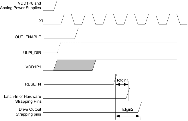 Figure 4-1 Power-Up and Reset Timing
Table 4-1 Power-Up and Reset Timing
| MIN | NOM | MAX | UNIT | ||
|---|---|---|---|---|---|
| Tcfgin1 | Hardware configuration latch-in time from RESETN | 0 | ns | ||
| Tcfgin2 | Time from RESETN to driver outputs on strapping pins | 0 | ns | ||
| RESETN pulse width | 1 | µs | |||
| RESETN to PHY_STATUS deassertion | 300 | µs | |||
4.7.2 PIPE Transmit
 Figure 4-2 PIPE Transmit Timing
Table 4-2 PIPE Transmit Timing
| MIN | NOM | MAX | UNIT | ||
|---|---|---|---|---|---|
| Tcyc2 | TX_CLK period | 4 | ns | ||
| Tdty2 | TX_CLK duty cycle | 50% | |||
| Tsu2 | Data setup to TX_CLK rise and TX_CLK fall(1) | 1 | ns | ||
| Thd2 | Data hold to TX_CLK rise and TX_CLK fall(1) | 0 | ns | ||
(1) This includes TX_DATA15-0, TX_DATAK1-0, TX_ONESZEROS, RATE, TX_DEEMPTH, TX_DETRX_LPBK, TX_ELECIDLE, TX_MARGIN, TX_SWING, RX_POLARITY, POWER_DOWN1-0.
4.7.3 PIPE Receive
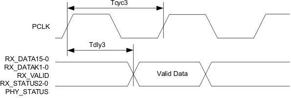 Figure 4-3 PIPE Receive Timing
Table 4-3 PIPE Receive Timing
| MIN | NOM | MAX | UNIT | ||
|---|---|---|---|---|---|
| Tcyc3 | PCLK Period | 4 | ns | ||
| Tdty3 | PCLK Duty Cycle | 50% | |||
| Tdly3 | PCLK rise and fall to RX_DATA15-0, RX_DATAK1-0, RX_VALID, RX_STATUS2-0, PHY_STATUS Delay(1)(2) | 1 | 2 | ns | |
(1) Output Load max = 10 pF, min = 5 pF
(2) Timing is relative to the 50% transition point, not VIH or VIL.
4.7.4 ULPI Parameters
Table 4-4 ULPI Parameters
| DESCRIPTION | NOTES | HS | FS | LS | UNIT |
|---|---|---|---|---|---|
| RX CMD delay | PHY pipeline delays | 2 to 4 | 2 to 4 | 2 to 4 | clocks |
| TX start delay | 1 to 2 | 1 to 10 | 1 to 10 | clocks | |
| TX end delay | 2 to 5 | clocks | |||
| RX start delay | 3 to 8 | clocks | |||
| RX end delay | 3 to 8 | 17 to 18 | 122 to 123 | clocks | |
| Transmit-Transmit (host only) | Link decision times | 15 to 24 | 7 to 18 | 77 to 247 | clocks |
| Receive-Transmit (host or peripheral) | 1 to 14 | 7 to 18 | 77 to 247 | clocks |
4.7.5 ULPI Clock
Table 4-5 ULPI Clock Parameters
| MIN | NOM | MAX | UNIT | ||
|---|---|---|---|---|---|
| Fstart_8bit | Frequency (first transition) ±10% | 54 | 60 | 66 | MHz |
| Fsteady | Frequency (steady state) ±500 ppm | 59.97 | 60 | 60.03 | MHz |
| Dstart_8bit | Duty cycle (first transition) ±10% | 40% | 50% | 60% | |
| Dsteady | Duty cycle (steady state) ±500 ppm | 49.975% | 50% | 50.025% | |
| Tsteady | Time to reach steady state frequency and duty cycle after first transition | 1.4 | ms | ||
| Tstart_dev | Clock startup time after deassertion of SuspemdM – Peripheral | 5.6 | ms | ||
| Tstart_host | Clock startup time after deassertion of SuspemdM – Hold | ms | |||
| Tprep | PHY preparation time after first transition of input clock | µs | |||
| Tjitter | Jitter | ps | |||
| Trise, Tfall | Rise and fall time | ns | |||
4.7.6 ULPI Transmit
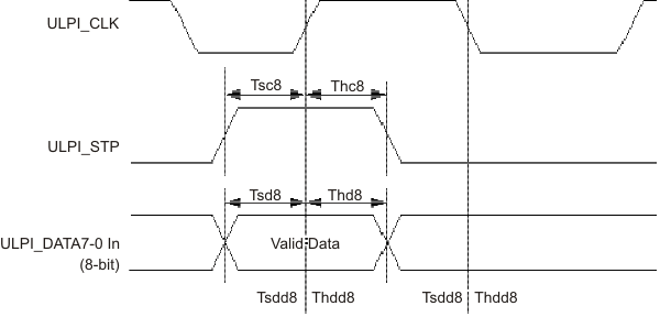 Figure 4-4 ULPI Transmit Timing
Table 4-6 ULPI Transmit Timing
| MIN | NOM | MAX | UNIT | ||
|---|---|---|---|---|---|
| Tsc8, Tsd8 | ULPI_STP set-up time | 6 | ns | ||
| Thc8, Thd8 | ULPI_STP hold time | 0 | ns | ||
4.7.7 ULPI Receive Timing
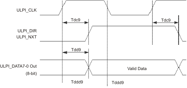 Figure 4-5 ULPI Receive Timing
Table 4-7 ULPI Receive Timing
| MIN | NOM | MAX | UNIT | ||
|---|---|---|---|---|---|
| Tdc9, Tdd9 | ULPI_DIR/ULPI_NXT/ULPI_DATA7-0(1) | 9 | ns | ||
(1) Output Load MAX = 10 pF, MIN = 5 pF
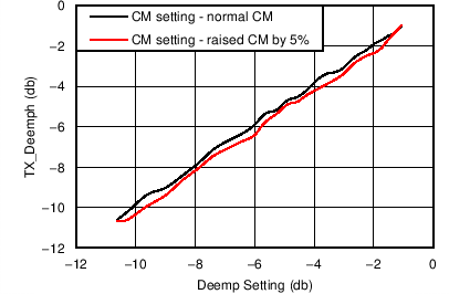
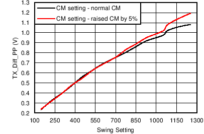
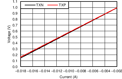
4.8 Typical Characteristics
