SLVS754D March 2007 – January 2015 TPS65053
PRODUCTION DATA.
- 1 Features
- 2 Applications
- 3 Description
- 4 Revision History
- 5 Pin Configuration and Functions
- 6 Specifications
-
7 Detailed Description
- 7.1 Overview
- 7.2 Functional Block Diagrams
- 7.3 Feature Description
- 7.4 Device Functional Modes
-
8 Application and Implementation
- 8.1 Application Information
- 8.2
Typical Application
- 8.2.1 Design Requirements
- 8.2.2 Detailed Design Procedure
- 8.2.3 Application Curves
- 9 Power Supply Recommendations
- 10Layout
- 11Device and Documentation Support
- 12Mechanical, Packaging, and Orderable Information
封裝選項(xiàng)
機(jī)械數(shù)據(jù) (封裝 | 引腳)
- RGE|24
散熱焊盤機(jī)械數(shù)據(jù) (封裝 | 引腳)
- RGE|24
訂購(gòu)信息
6 Specifications
6.1 Absolute Maximum Ratings
over operating free-air temperature range (unless otherwise noted)(1)(1) Stresses beyond those listed under Absolute Maximum Ratings may cause permanent damage to the device. These are stress ratings only and functional operation of the device at these or any other conditions beyond those indicated under Recommended Operating Conditions is not implied. Exposure to absolute-maximum-rated conditions for extended periods may affect device reliability.
6.2 ESD Ratings
| VALUE | UNIT | |||
|---|---|---|---|---|
| V(ESD) | Electrostatic discharge | Human-body model (HBM), per ANSI/ESDA/JEDEC JS-001(1) | ±2000 | V |
| Charged-device model (CDM), per JEDEC specification JESD22-C101(2) | ±500 | |||
(1) JEDEC document JEP155 states that 500-V HBM allows safe manufacturing with a standard ESD control process. Manufacturing with less than 500-V HBM is possible with the necessary precautions.
(2) JEDEC document JEP157 states that 250-V CDM allows safe manufacturing with a standard ESD control process. Manufacturing with less than 250-V CDM is possible with the necessary precautions.
6.3 Recommended Operating Conditions
| MIN | NOM | MAX | UNIT | ||
|---|---|---|---|---|---|
| VINDCDC1/2 | Input voltage range for step-down converters | 2.5 | 6 | V | |
| VDCDC1 | Output voltage range for VDCDC1 step-down converter for externally adjustable versions | 0.6 | VINDCDC1 | V | |
| VDCDC2 | Output voltage range for VDCDC2 step-down converter for externally adjustable versions | 0.6 | VINDCDC2 | V | |
| VINLDO1, VINLDO2/3 | Input voltage range for LDOs | 1.5 | 6.5 | V | |
| VLDO1-2 | Output voltage range for LDO1 and LDO2 for externally adjustable versions | 1 | 3.6 | V | |
| Output voltage for LDO1 on TPS65058 | 3.3 | V | |||
| Output voltage for LDO2 on TPS65058 (DEF_LDO = 1 / 0) | 1.8 / 1.2 | V | |||
| VLDO3 | Output voltage for LDO3 on TPS65053 | 1.3 | V | ||
| Output voltage for LDO3 on TPS650531 | 1.2 | ||||
| Output voltage for LDO3 on TPS650532 | 1.5 | ||||
| Output voltage for LDO3 on TPS65058 (DEF_LDO = 1 / 0) | 1.8 / 1.3 | V | |||
| IOUTDCDC1 | Output current at L1 for TPS65053, TPS650531, TPS650532 | 1000 | mA | ||
| Output current at L1 for TPS65058 | 600 | mA | |||
| L1 | Inductor at L1(1) | 1.5 | 2.2 | μH | |
| CINDCDC1/2 | Input capacitor at VINDCDC1/2(1) | 22 | μF | ||
| COUTDCDC1 | Output capacitor at VDCDC1(1) | 10 | 22 | μF | |
| IOUTDCDC2 | Output current at L2 for TPS65053 | 600 | mA | ||
| Output current at L2 for TPS650531, TPS650532, TPS65058 | 1000 | ||||
| L2 | Inductor at L2(1) | 1.5 | 2.2 | μH | |
| COUTDCDC2 | Output capacitor at VDCDC2(1) | 10 | 22 | μF | |
| CVCC | Input capacitor at VCC (1) | 1 | μF | ||
| Cin1-2 | Input capacitor at VINLDO1, VINLDO2/3 (1) | 2.2 | μF | ||
| COUT1 | Output capacitor at VLDO1 (1) | 4.7 | μF | ||
| COUT2-3 | Output capacitor at VLDO2-3 (1) | 2.2 | μF | ||
| ILDO1 | Output current at VLDO1 | 400 | mA | ||
| ILDO2,3 | Output current at VLDO2,3 | 200 | mA | ||
| TA | Operating ambient temperature range | –40 | 85 | °C | |
| TJ | Operating junction temperature range | –40 | 125 | °C | |
| RCC | Resistor from battery voltage to VCC used for filtering(2) | 1 | 10 | Ω | |
(1) See the Application Information section of this data sheet for more details.
(2) Up to 2 mA can flow into VCC when both converters are running in PWM, this resistor causes the UVLO threshold to be shifted accordingly.
6.4 Thermal Information
| THERMAL METRIC(1) | TPS65053 | UNIT | |
|---|---|---|---|
| VQFN | |||
| 24 PINS | |||
| RθJA | Junction-to-ambient thermal resistance | 31.4 | °C/W |
| RθJC(top) | Junction-to-case (top) thermal resistance | 29.0 | |
| RθJB | Junction-to-board thermal resistance | 8.2 | |
| ψJT | Junction-to-top characterization parameter | 0.3 | |
| ψJB | Junction-to-board characterization parameter | 8.2 | |
| RθJC(bot) | Junction-to-case (bottom) thermal resistance | 1.6 | |
(1) For more information about traditional and new thermal metrics, see the IC Package Thermal Metrics application report, SPRA953.
6.5 Dissipation Ratings
| PACKAGE | RθJA(1) | TA ≤ 25°C POWER RATING |
DERATING FACTOR ABOVE TA = 25°C |
TA = 70°C POWER RATING |
TA = 85°C POWER RATING |
|---|---|---|---|---|---|
| RGE | 35 K/W | 2.8 W | 28 mW/K | 1.57 W | 1.14 W |
(1) The thermal resistance junction to case of the RGE package is 2 K/W measured on a high K board.
6.6 Electrical Characteristics
Vcc = VINDCDC1/2 = 3.6V, EN = Vcc, MODE = GND, L = 2.2μH, COUT = 22μF, TA = –40°C to 85°C typical valuesare at TA = 25°C (unless otherwise noted).
| PARAMETER | TEST CONDITIONS | MIN | TYP | MAX | UNIT | |||
|---|---|---|---|---|---|---|---|---|
| SUPPLY CURRENT | ||||||||
| Vcc | Input voltage range | 2.5 | 6 | V | ||||
| IQ | Operating quiescent current Total current into VCC, VINDCDC1/2, VINLDO1, VINLDO2/3 |
One converter, IOUT = 0 mA.PFM mode enabled (Mode = GND) device not switching, EN_DCDC1 = Vin OR EN_DCDC2 = Vin; EN_LDO1= EN_LDO2 = EN_LDO3 = GND |
20 | 30 | μA | |||
| Two converters, IOUT = 0 mA, PFM mode enabled (Mode = 0) device not switching, EN_DCDC1 = Vin AND EN_DCDC2 = Vin; EN_LDO1 = EN_LDO2 = EN_LDO3 = GND |
32 | 40 | μA | |||||
| One converter, IOUT = 0 mA, PFM mode enabled (Mode = GND) device not switching, EN_DCDC1 = Vin OR EN_DCDC2 = Vin; EN_LDO1 = EN_LDO2 = EN_LDO3 = Vin |
145 | 210 | μA | |||||
| IQ | Operating quiescent current into VCC | One converter, IOUT = 0 mA, Switching with no load (Mode = Vin), PWM operation EN_DCDC1 = Vin OR EN_DCDC2 = Vin; EN_LDO1 = EN_LDO2 = EN_LDO3 = GND |
0.85 | mA | ||||
| Two converters, IOUT = 0 mA, Switching with no load (Mode = Vin), PWM operation EN_DCDC1 = Vin AND EN_DCDC2 = Vin; EN_LDO1 = EN_LDO2 = EN_LDO3 = GND |
1.25 | mA | ||||||
| I(SD) | Shutdown current | EN_DCDC1 = EN_DCDC2 = GND EN_LDO1 = EN_LDO2 = EN_LDO3 = GND |
9 | 12 | μA | |||
| UVLO | Undervoltage lockout threshold for DCDC converters and LDOs | Voltage at VCC | 1.8 | 2 | V | |||
| EN_DCDC1, EN_DCDC2, EN_LDO1, EN_LDO2, EN_LDO3, MODE | ||||||||
| VIH | High-level input voltage | MODE, EN_DCDC1, EN_DCDC2, EN_LDO1, EN_LDO2, EN_LDO3 | 1.2 | VCC | V | |||
| VIL | Low-level input voltage | MODE, EN_DCDC1, EN_DCDC2, EN_LDO1, EN_LDO2, EN_LDO3 | 0 | 0.4 | V | |||
| IIN | Input bias current | MODE, EN_DCDC1, EN_DCDC2, EN_LDO1, EN_LDO2, EN_LDO3, MODE = GND or VIN | 0.01 | 1 | μA | |||
| POWER SWITCH | ||||||||
| rDS(on) High Side | P-channel MOSFET on resistance for TPS65053, TPS650531, TPS650532 | DCDC1, DCDC2 | VINDCDC1/2 = 3.6 V | 280 | 630 | mΩ | ||
| VINDCDC1/2 = 2.5 V | 400 | |||||||
| P-channel MOSFET on resistance for TPS65058 | DCDC1, DCDC2 | VINDCDC1/2 = 3.6 V | 250 | 350 | mΩ | |||
| VINDCDC1/2 = 2.5 V | 380 | 500 | ||||||
| ILD_PMOS | P-channel leakage current | V(DS) = 6 V | 1 | μA | ||||
| rDS(on) Low-Side | N-channel MOSFET on resistance for TPS65053, TPS650531, TPS650532 | DCDC1, DCDC2 | VINDCDC1/2 = 3.6 V | 220 | 450 | mΩ | ||
| VINDCDC1/2 = 2.5 V | 320 | |||||||
| N-channel MOSFET on resistance for TPS65058 | DCDC1, DCDC2 | VINDCDC1/2 = 3.6 V | 180 | 250 | mΩ | |||
| VINDCDC1/2 = 2.5 V | 250 | |||||||
| ILK_NMOS | N-channel leakage current | V(DS) = 6 V | 7 | 10 | μA | |||
| I(LIMF) | Forward Current Limit PMOS (High-Side) and NMOS (Low side) | DCDC1 (TPS65053, TPS650531, TPS650532) | 2.5 V ≤ VIN ≤ 6 V | 1.19 | 1.4 | 1.65 | A | |
| DCDC1 (TPS65058) | 0.85 | 1 | 1.15 | |||||
| DCDC2 (TPS65053) | 0.85 | 1 | 1.15 | |||||
| DCDC2 (TPS650531, TPS650532, TPS65058) | 1.19 | 1.4 | 1.65 | |||||
| TSD | Thermal shutdown | Increasing junction temperature | 150 | °C | ||||
| Thermal shutdown hysteresis | Decreasing junction temperature | 20 | °C | |||||
| OSCILLATOR | ||||||||
| fSW | Oscillator frequency | 2.025 | 2.25 | 2.475 | MHz | |||
| OUTPUT | ||||||||
| VOUT | Output voltage range for externally adjustable versions | 0.6 | VIN | V | ||||
| Vref | Reference voltage | 600 | mV | |||||
| VOUT | DC output voltage accuracy | DCDC1, DCDC2(1) | VIN = 2.5 V to 6 V, Mode = GND, PFM operation, 0 mA < IOUT < IOUTMAX |
-2% | 0 | 2% | ||
| VIN = 2.5 V to 6 V, Mode = VIN, PWM operation, 0 mA < IOUT < IOUTMAX |
–1% | 0 | 1% | |||||
| ΔVOUT | Power save mode ripple voltage(2) | IOUT = 1 mA, Mode = GND, VO = 1.3 V, Bandwidth = 20 MHz |
25 | mVPP | ||||
| tStart | Start-up time | Time from active EN to Start switching | 170 | μs | ||||
| tRamp | VOUT Ramp up Time | Time to ramp from 5% to 95% of VOUT | 750 | μs | ||||
| RESET delay time | Input voltage at threshold pin rising | 80 | 100 | 120 | ms | |||
| VOL | RESET output low voltage | IOL = 1 mA, Vthreshold < 1 V | 0.2 | V | ||||
| RESET sink current | 1 | mA | ||||||
| RESET output leakage current | (Vthreshold > 1 V for TPS65053, TPS650531, TPS650532) | 10 | nA | |||||
| Vth | Threshold voltage TPS65053, TPS650531, TPS650532 | falling voltage | 0.98 | 1 | 1.02 | V | ||
| VLDO1, VLDO2, VLDO3 LOW DROPOUT REGULATORS | ||||||||
| VINLDO | Input voltage range for LDO1, LDO2, LDO3 | 1.5 | 6.5 | V | ||||
| VLDO1 | LDO1 output voltage range for TPS65053, TPS650531, TPS650532 | 1 | 3.6 | V | ||||
| LDO1 output voltage for TPS65058 | 3.3 | V | ||||||
| VLDO2 | LDO2 output voltage range for TPS65053, TPS650531, TPS650532 | 1 | 3.6 | V | ||||
| LDO2 output voltage for TPS65058 | DEF_LDO = 1 / 0 | 1.8 / 1.2 | V | |||||
| VLDO3 | LDO3 output voltage for TPS65053 | 1.3 | V | |||||
| LDO3 output voltage for TPS650531 | 1.2 | |||||||
| LDO3 output voltage for TPS650532 | 1.5 | |||||||
| LDO3 output voltage for TPS65058 | DEF_LDO = 1 / 0 | 1.8 / 1.3 | ||||||
| V(FB) | Feedback voltage for FB_LDO1, FB_LDO2 | for externally adjustable versions | 1 | V | ||||
| IO | Maximum output current for LDO1 | 400 | mA | |||||
| Maximum output current for LDO2, LDO3 | 200 | mA | ||||||
| I(SC) | LDO1 short-circuit current limit | VLDO1 = GND | 850 | mA | ||||
| LDO2 & LDO3 short-circuit current limit | VLDO2 = GND, VLDO3 = GND | 420 | mA | |||||
| Dropout voltage at LDO1 | IO = 400 mA, VINLDO1 = 1.8 V | 280 | mV | |||||
| Dropout voltage at LDO2, LDO3 | IO = 200 mA, VINLDO2/3 = 1.8 V | 280 | mV | |||||
| Output voltage accuracy for LDO1, LDO2, LDO3(1) | IO = 10 mA | –2% | 1% | |||||
| Line regulation for LDO1, LDO2, LDO3 | VINLDO1,2 = VLDO1,2 + 0.5 V (min. 2.5 V) to 6.5V, IO = 10 mA | –1% | 1% | |||||
| Load regulation for LDO1, LDO2, LDO3 | IO = 0 mA to 400 mA for LDO1 IO = 0 mA to 200 mA for LDO2, LDO3 |
–1% | 1% | |||||
| Regulation time for LDO1, LDO2, LDO3 | Load change from 10% to 90% | 25 | μs | |||||
| Regulation time for LDO1, LDO2, LDO3 for TPS65058 | Load change from 10% to 90% | 10 | μs | |||||
| PSRR | Power Supply Rejection Ratio | f = 10 kHz; IO = 50 mA; VI = VO + 1 V | ||||||
| R(DIS) | Internal discharge resistor at VLDO1, VLDO2, VLDO3 | Active when LDO is disabled | 350 | Ω | ||||
| Internal discharge resistor at VLDO1, VLDO2, VLDO3 for TPS65058 | Active when LDO is disabled | 300 | Ω | |||||
| Thermal shutdown | Increasing junction temperature | 140 | °C | |||||
| Thermal shutdown hysteresis | Decreasing junction temperature | 20 | °C | |||||
(1) Output voltage specification does not include tolerance of external voltage programming resistors.
(2) In Power Save Mode, operation is typically entered at IPSM = VIN / 32 Ω.
6.7 Typical Characteristics
Table 1. Table Of Graphs for TPS6505xx
| FIGURE | |||
|---|---|---|---|
| η | Efficiency converter 1 | vs Load current PWM/PFM mode | Figure 1 |
| η | Efficiency converter 1 | vs Load current PWM mode | Figure 2 |
| η | Efficiency converter 2 | vs Load current PWM/PFM mode | Figure 3 |
| η | Efficiency converter 2 | vs Load current PWM mode | Figure 4 |
| Output voltage ripple in PFM mode | Scope plot | Figure 5 | |
| Output voltage ripple in PWM mode | Scope plot | Figure 6 | |
| DCDC1, DCDC2, LDO1 startup timing | Scope plot | Figure 7 | |
| LDO1 to LDO3 startup timing | Scope plot | Figure 8 | |
| DCDC1 Load transient response in PWM mode | Scope plot | Figure 9 | |
| DCDC1 Load transient response in PFM mode | Scope plot | Figure 10 | |
| DCDC2 Load transient response in PWM mode | Scope plot | Figure 11 | |
| DCDC2 Load transient response in PFM mode | Scope plot | Figure 12 | |
| DCDC1 Line transient response in PWM mode | Scope plot | Figure 13 | |
| DCDC2 Line transient response in PWM mode | Scope plot | Figure 14 | |
| LDO1 Load transient response | Scope plot | Figure 15 | |
| LDO3 Load transient response | Scope plot | Figure 16 | |
| LDO1 Line transient response | Scope plot | Figure 17 | |
| LDO1 Power supply rejection ratio | vs frequency | Figure 18 | |
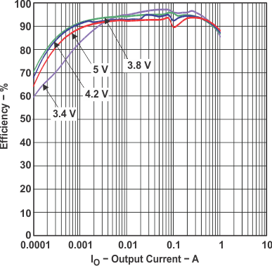 Figure 1. Efficiency vs Output Current
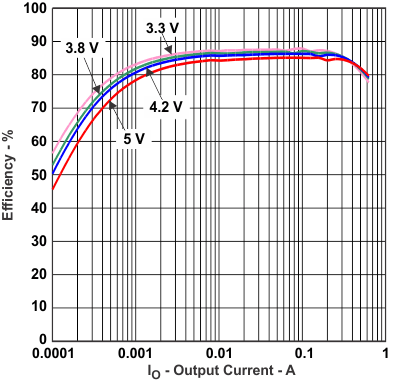 Figure 3. Efficiency vs Output Current
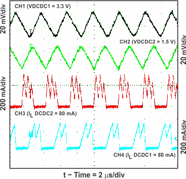 Figure 5. Output Voltage Ripple PWM/PFM Mode = Low
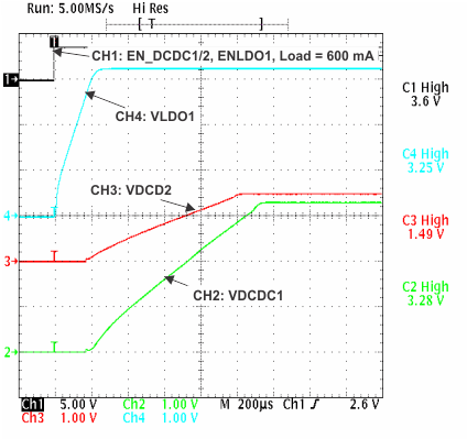 Figure 7. DCDC1 Startup Timing
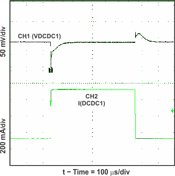 Figure 9. DCDC1 Load Transient Response
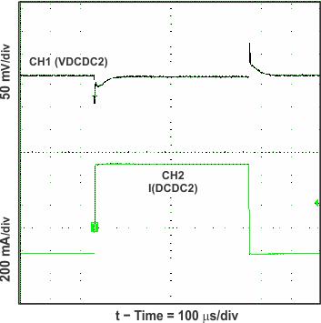 Figure 11. DCDC2 Load Transient Response
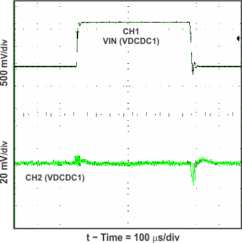 Figure 13. DCDC1 Line Transient Response
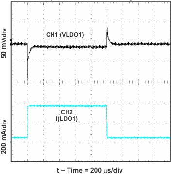 Figure 15. LDO1 Load Transient Response
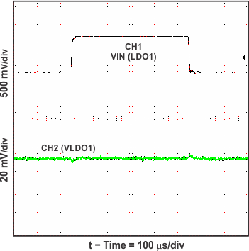 Figure 17. LDO1 Line Transient Response
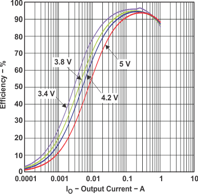 Figure 2. Efficiency vs Output Current
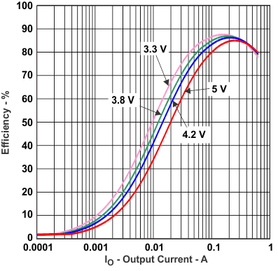 Figure 4. Efficiency vs Output Current
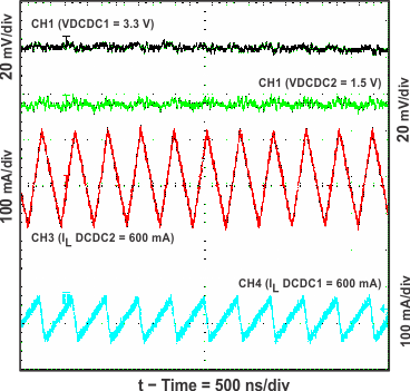 Figure 6. Output Voltage Ripple PWM Mode = High
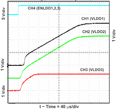 Figure 8. LDO1 to LDO3 Startup Timing
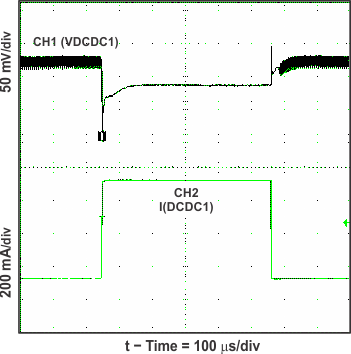 Figure 10. DCDC1 Load Transient Response
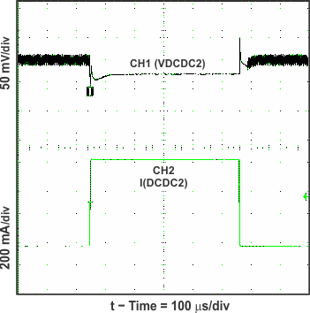 Figure 12. DCDC2 Load Transient Response
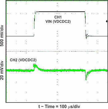 Figure 14. DCDC2 Line Transient Response
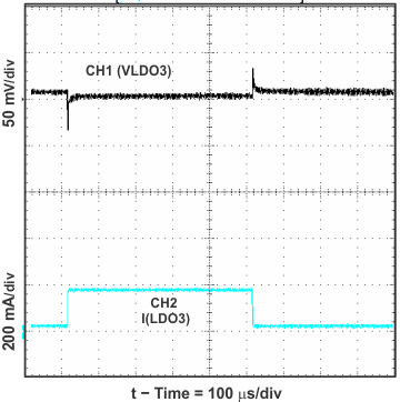 Figure 16. LDO3 Load Transient Response
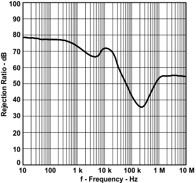 Figure 18. LDO1 Power Supply Rejection Ratio vs Frequency