ZHCSFX0B November 2016 – August 2017 TLV2316-Q1 , TLV316-Q1 , TLV4316-Q1
PRODUCTION DATA.
- 1 特性
- 2 應(yīng)用
- 3 說明
- 4 修訂歷史記錄
- 5 Device Comparison Table
- 6 Pin Configuration and Functions
- 7 Specifications
- 8 Detailed Description
- 9 Application and Implementation
- 10Power Supply Recommendations
- 11Layout
- 12器件和文檔支持
- 13機械、封裝和可訂購信息
封裝選項
機械數(shù)據(jù) (封裝 | 引腳)
- DBV|5
散熱焊盤機械數(shù)據(jù) (封裝 | 引腳)
訂購信息
7 Specifications
7.1 Absolute Maximum Ratings
over operating free-air temperature (unless otherwise noted)(1)| MIN | MAX | UNIT | |||
|---|---|---|---|---|---|
| Supply voltage | 7 | V | |||
| Signal input pins | Voltage(2) | Common-mode | (V–) – 0.5 | (V+) + 0.5 | V |
| Differential | (V+) – (V–) + 0.2 | ||||
| Current(2) | –10 | 10 | mA | ||
| Output short-circuit(3) | Continuous | mA | |||
| Temperature | Specified, TA | –40 | 125 | °C | |
| Junction, TJ | 150 | ||||
| Storage, Tstg | –65 | 150 | |||
(1) Stresses beyond those listed under Absolute Maximum Ratings may cause permanent damage to the device. These are stress ratings only, and functional operation of the device at these or any other conditions beyond those indicated under Recommended Operating Conditions is not implied. Exposure to absolute-maximum-rated conditions for extended periods may affect device reliability.
(2) Input pins are diode-clamped to the power-supply rails. Current limit input signals that can swing more than 0.5 V beyond the supply rails to 10 mA or less.
(3) Short-circuit to ground, one amplifier per package.
7.2 ESD Ratings
| VALUE | UNIT | |||
|---|---|---|---|---|
| V(ESD) | Electrostatic discharge | Human-body model (HBM), per AEC Q100-002(1) | ±4000 | V |
| Charged-device model (CDM), per AEC Q100-011 | ±750 | |||
(1) AEC Q100-002 indicates that HBM stressing shall be in accordance with the ANSI/ESDA/JEDEC JS-001 specification.
7.3 Recommended Operating Conditions
over operating free-air temperature range (unless otherwise noted)| MIN | NOM | MAX | UNIT | |||
|---|---|---|---|---|---|---|
| VS | Supply voltage | 1.8 | 5.5 | V | ||
| Specified temperature range | –40 | 125 | °C | |||
7.4 Thermal Information: TLV316-Q1
| THERMAL METRIC(1) | TLV316-Q1 | UNIT | |
|---|---|---|---|
| DBV (SOT-23) | |||
| 5 PINS | |||
| RθJA | Junction-to-ambient thermal resistance | 221.7 | °C/W |
| RθJC(top) | Junction-to-case(top) thermal resistance | 144.7 | °C/W |
| RθJB | Junction-to-board thermal resistance | 49.7 | °C/W |
| ψJT | Junction-to-top characterization parameter | 26.1 | °C/W |
| ψJB | Junction-to-board characterization parameter | 49.0 | °C/W |
| RθJC(bot) | Junction-to-case(bottom) thermal resistance | N/A | °C/W |
(1) For more information about traditional and new thermal metrics, see the Semiconductor and IC Package Thermal Metrics application report.
7.5 Thermal Information: TLV2316-Q1
| THERMAL METRIC(1) | TLV2316-Q1 | UNIT | |
|---|---|---|---|
| DGK (VSSOP) | |||
| 8 PINS | |||
| RθJA | Junction-to-ambient thermal resistance | 186.6 | °C/W |
| RθJC(top) | Junction-to-case(top) thermal resistance | 78.8 | °C/W |
| RθJB | Junction-to-board thermal resistance | 107.9 | °C/W |
| ψJT | Junction-to-top characterization parameter | 15.5 | °C/W |
| ψJB | Junction-to-board characterization parameter | 106.3 | °C/W |
| RθJC(bot) | Junction-to-case(bottom) thermal resistance | N/A | °C/W |
(1) For more information about traditional and new thermal metrics, see the Semiconductor and IC Package Thermal Metrics application report.
7.6 Thermal Information: TLV4316-Q1
| THERMAL METRIC(1) | TLV4316-Q1 | UNIT | |
|---|---|---|---|
| PW (TSSOP) | |||
| 14 PINS | |||
| RθJA | Junction-to-ambient thermal resistance | 117.8 | °C/W |
| RθJC(top) | Junction-to-case(top) thermal resistance | 46.5 | °C/W |
| RθJB | Junction-to-board thermal resistance | 59.6 | °C/W |
| ψJT | Junction-to-top characterization parameter | 5.3 | °C/W |
| ψJB | Junction-to-board characterization parameter | 59 | °C/W |
| RθJC(bot) | Junction-to-case(bottom) thermal resistance | N/A | °C/W |
(1) For more information about traditional and new thermal metrics, see the Semiconductor and IC Package Thermal Metrics application report.
7.7 Electrical Characteristics
at TA = 25°C, RL = 10 kΩ connected to VS / 2, VCM = VS / 2, and VOUT = VS / 2 (unless otherwise noted); VS (total supply voltage) = (V+) – (V–) = 1.8 V to 5.5 V| PARAMETER | TEST CONDITIONS | MIN | TYP | MAX | UNIT | ||
|---|---|---|---|---|---|---|---|
| OFFSET VOLTAGE | |||||||
| VOS | Input offset voltage | VS = 5 V | ±0.75 | ±3 | mV | ||
| VS = 5 V, TA = –40°C to 125°C | ±4.5 | ||||||
| dVOS/dT | Drift | VS = 5 V, TA = –40°C to 125°C | ±2 | µV/°C | |||
| PSRR | Power-supply rejection ratio | VS = 1.8 V – 5.5 V, VCM = (V–) | ±30 | ±175 | µV/V | ||
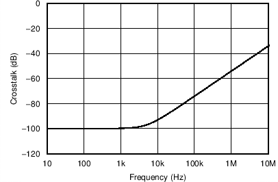
| Channel separation, dc | At dc | 100 | dB | ||||
| INPUT VOLTAGE RANGE | |||||||
| VCM | Common-mode voltage range | VS = 5.5 V | (V–) – 0.2 | (V+) + 0.2 | V | ||
| CMRR | Common-mode rejection ratio | VS = 5.5 V, (V–) – 0.2 V < VCM < (V+) – 1.4 V, TA = –40°C to 125°C |
72 | 90 | dB | ||
| VS = 5.5 V, VCM = –0.2 V to 5.7 V, TA = –40°C to 125°C |
75 | ||||||
| INPUT BIAS CURRENT | |||||||
| IB | Input bias current | ±10 | pA | ||||
| IOS | Input offset current | ±10 | pA | ||||
| NOISE | |||||||
| En | Input voltage noise (peak-to-peak) | VS = 5 V, f = 0.1 Hz to 10 Hz | 5 | µVPP | |||
| en | Input voltage noise density | VS = 5 V, f = 1 kHz | 12 | nV/√Hz | |||
| in | Input current noise density | f = 1 kHz | 1.3 | fA/√Hz | |||
| INPUT IMPEDANCE | |||||||
| ZID | Differential | 2 || 2 | 1016Ω || pF | ||||
| ZIC | Common-mode | 2 || 4 | 1011Ω || pF | ||||
| OPEN-LOOP GAIN | |||||||
| AOL | Open-loop voltage gain | VS = 5.5 V, (V–) + 0.05 V < VO < (V+) – 0.05 V, RL = 10 kΩ |
100 | 104 | dB | ||
| VS = 5.5 V, (V–) + 0.15 V < VO < (V+) – 0.15 V, RL = 2 kΩ |
104 | ||||||
| FREQUENCY RESPONSE | |||||||
| GBP | Gain bandwidth product | VS = 5 V, G = 1 | 10 | MHz | |||
| φm | Phase margin | VS = 5 V, G = 1 | 60 | Degrees | |||
| SR | Slew rate | VS = 5 V, G = 1 | 6 | V/μs | |||
| tS | Settling time | To 0.1%, VS = 5 V, 2-V step , G = 1, CL = 100 pF | 1 | μs | |||
| tOR | Overload recovery time | VS = 5 V, VIN × gain = VS | 0.8 | μs | |||
| THD + N | Total harmonic distortion + noise(1) | VS = 5 V, VO = 0.5 VRMS, G = 1, f = 1 kHz | 0.008% | ||||
| OUTPUT | |||||||
| VO | Voltage output swing from supply rails | VS = 1.8 V to 5.5 V, RL = 10 kΩ | 35 | mV | |||
| VS = 1.8 to 5.5 V, RL = 2 kΩ | 125 | ||||||
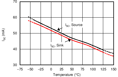
| ISC | Short-circuit current | VS = 5 V | ±50 | mA | |||
| ZO | Open-loop output impedance | VS = 5 V, f = 10 MHz | 250 | Ω | |||
| POWER SUPPLY | |||||||
| VS | Specified voltage range | 1.8 | 5.5 | V | |||
| IQ | Quiescent current per amplifier | VS = 5 V, IO = 0 mA, TA = –40°C to 125°C | 400 | 575 | µA | ||
| TEMPERATURE | |||||||
| TA | Specified | –40 | 125 | °C | |||
| Tstg | Storage | –65 | 150 | °C | |||
(1) Third-order filter; bandwidth = 80 kHz at –3 dB.
7.8 Typical Characteristics: Table of Graphs
Table 1. Table of Graphs
| TITLE | FIGURE |
|---|---|
| Offset Voltage Production Distribution | Figure 1 |
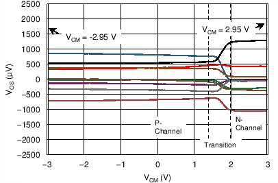
| Offset Voltage vs Common-Mode Voltage | Figure 2 |
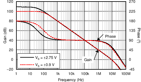
| Open- Loop Gain and Phase vs Frequency | Figure 3 |
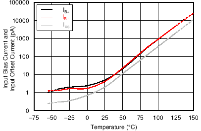
| Input Bias and Offset Current vs Temperature | Figure 4 |
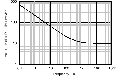
| Input Voltage Noise Spectral Density vs Frequency | Figure 5 |
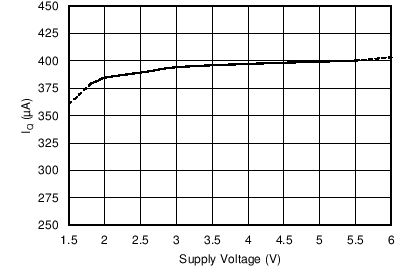
| Quiescent Current vs Supply Voltage | Figure 6 |
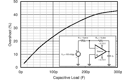
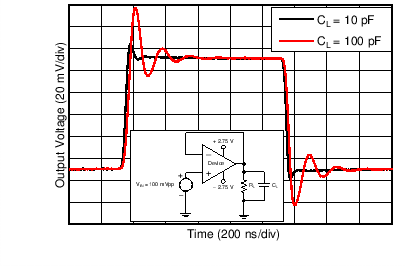
| Small-Signal Overshoot vs Load Capacitance | Figure 7 |
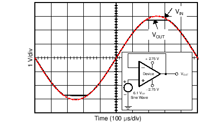
| No Phase Reversal | Figure 8 |
| Small-Signal Step Response | Figure 9 |
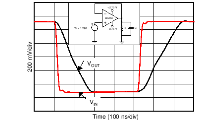
| Large-Signal Step Response | Figure 10 |
| Short-Circuit Current vs Temperature | Figure 11 |
| Electromagnetic Interference Rejection Ratio Referred to Noninverting Input vs Frequency | Figure 12 |
| Channel Separation vs Frequency | Figure 13 |
7.9 Typical Characteristics
at TA = 25°C, VS = 5.5 V, RL = 10 kΩ connected to VS / 2, VCM = VS / 2, and VOUT = VS / 2, (unless otherwise noted)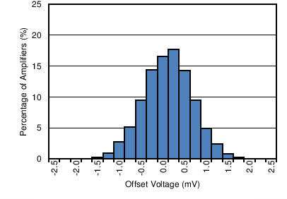
| Distribution taken from 12551 amplifiers |
| VCM < (V+) – 1.4 V | ||
| V+ = 2.75 V, V– = –2.75 V, G = –1 V/V | ||
| V+ = 2.75 V, V– = –2.75 V, G = 1 V/V | ||
| V+ = 2.75 V, V– = –2.75 V | ||
| V+ = 2.75 V | V– = –2.75 V | 9 typical units shown |
| V+ = 2.75 V, V– = –2.75 V | ||
| V+ = 2.75 V, V– = –2.75 V, CL = 100 pF, G = 1 V/V | ||
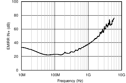
| PRF = –10 dBm | ||
Referred to Noninverting Input vs Frequency