SNAS805 June 2020 LMK61E08
PRODUCTION DATA.
- 1 Features
- 2 Applications
- 3 Description
- 4 Revision History
- 5 Pin Configuration and Functions
-
6 Specifications
- 6.1 Absolute Maximum Ratings
- 6.2 ESD Ratings
- 6.3 Recommended Operating Conditions
- 6.4 Thermal Information
- 6.5 Electrical Characteristics - Power Supply
- 6.6 LVPECL Output Characteristics
- 6.7 LVDS Output Characteristics
- 6.8 HCSL Output Characteristics
- 6.9 Frequency Tolerance Characteristics
- 6.10 Frequency Margining Characteristics
- 6.11 Power-On Reset Characteristics (VDD)
- 6.12 I2C-Compatible Interface Characteristics (SDA, SCL)
- 6.13 PSRR Characteristics
- 6.14 Other Characteristics
- 6.15 PLL Clock Output Jitter Characteristics
- 6.16 Typical 156.25-MHz Output Phase Noise Characteristics
- 6.17 Typical 161.1328125 MHz Output Phase Noise Characteristics
- 6.18 Additional Reliability and Qualification
- 6.19 Typical Characteristics
- 7 Parameter Measurement Information
-
8 Detailed Description
- 8.1 Overview
- 8.2 Functional Block Diagram
- 8.3
Feature Description
- 8.3.1 Device Block-Level Description
- 8.3.2 Device Configuration Control
- 8.3.3 Register File Reference Convention
- 8.3.4 Configuring the PLL
- 8.3.5 Integrated Oscillator
- 8.3.6 Reference Divider and Doubler
- 8.3.7 Phase Frequency Detector
- 8.3.8 Feedback Divider (N)
- 8.3.9 Fractional Engine
- 8.3.10 Charge Pump
- 8.3.11 Loop Filter
- 8.3.12 VCO Calibration
- 8.3.13 High-Speed Output Divider
- 8.3.14 High-Speed Clock Output
- 8.3.15 Device Status
- 8.4 Device Functional Modes
- 8.5 Programming
- 8.6
Register Maps
- 8.6.1
Register Descriptions
- 8.6.1.1 VNDRID_BY1 Register; R0
- 8.6.1.2 VNDRID_BY0 Register; R1
- 8.6.1.3 PRODID Register; R2
- 8.6.1.4 REVID Register; R3
- 8.6.1.5 SLAVEADR Register; R8
- 8.6.1.6 EEREV Register; R9
- 8.6.1.7 DEV_CTL Register; R10
- 8.6.1.8 XO_CAPCTRL_BY1 Register; R16
- 8.6.1.9 XO_CAPCTRL_BY0 Register; R17
- 8.6.1.10 DIFFCTL Register; R21
- 8.6.1.11 OUTDIV_BY1 Register; R22
- 8.6.1.12 OUTDIV_BY0 Register; R23
- 8.6.1.13 RDIVCMOSCTL Register; R24
- 8.6.1.14 PLL_NDIV_BY1 Register; R25
- 8.6.1.15 PLL_NDIV_BY0 Register; R26
- 8.6.1.16 PLL_FRACNUM_BY2 Register; R27
- 8.6.1.17 PLL_FRACNUM_BY1 Register; R28
- 8.6.1.18 PLL_FRACNUM_BY0 Register; R29
- 8.6.1.19 PLL_FRACDEN_BY2 Register; R30
- 8.6.1.20 PLL_FRACDEN_BY1 Register; R31
- 8.6.1.21 PLL_FRACDEN_BY0 Register; R32
- 8.6.1.22 PLL_MASHCTRL Register; R33
- 8.6.1.23 PLL_CTRL0 Register; R34
- 8.6.1.24 PLL_CTRL1 Register; R35
- 8.6.1.25 PLL_LF_R2 Register; R36
- 8.6.1.26 PLL_LF_C1 Register; R37
- 8.6.1.27 PLL_LF_R3 Register; R38
- 8.6.1.28 PLL_LF_C3 Register; R39
- 8.6.1.29 PLL_CALCTRL Register; R42
- 8.6.1.30 NVMSCRC Register; R47
- 8.6.1.31 NVMCNT Register; R48
- 8.6.1.32 NVMCTL Register; R49
- 8.6.1.33 NVMLCRC Register; R50
- 8.6.1.34 MEMADR Register; R51
- 8.6.1.35 NVMDAT Register; R52
- 8.6.1.36 RAMDAT Register; R53
- 8.6.1.37 NVMUNLK Register; R56
- 8.6.1.38 INT_LIVE Register; R66
- 8.6.1.39 SWRST Register; R72
- 8.6.1
Register Descriptions
- 9 Application and Implementation
- 10Power Supply Recommendations
- 11Layout
- 12Device and Documentation Support
- 13Mechanical, Packaging, and Orderable Information
封裝選項(xiàng)
機(jī)械數(shù)據(jù) (封裝 | 引腳)
- SIA|6
散熱焊盤機(jī)械數(shù)據(jù) (封裝 | 引腳)
訂購(gòu)信息
7.1 Device Output Configurations
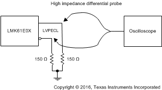 Figure 16. LVPECL Output DC Configuration During Device Test
 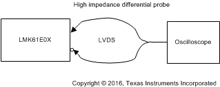 Figure 17. LVDS Output DC Configuration During Device Test
 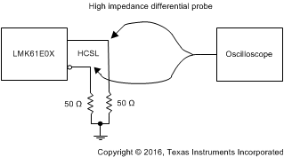 Figure 18. HCSL Output DC Configuration During Device Test
 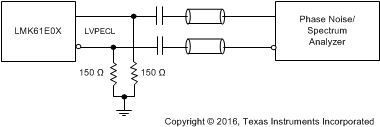 Figure 19. LVPECL Output AC Configuration During Device Test
  Figure 20. LVDS Output AC Configuration During Device Test
 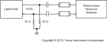 Figure 21. HCSL Output AC Configuration During Device Test
 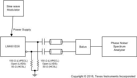 Figure 22. PSRR Test Setup
  Figure 23. Differential Output Voltage and Rise/Fall Time