ZHCSLQ5D October 2007 – August 2020 LM5067
PRODUCTION DATA
- 1 特性
- 2 應(yīng)用
- 3 說(shuō)明
- 4 Revision History
- 5 Device Comparison
- 6 Pin Configuration and Functions
- 7 Specifications
- 8 Detailed Description
-
9 Application and Implementation
- 9.1 Application Information
- 9.2
Typical Application
- 9.2.1 Design Requirements
- 9.2.2 Detailed Design Procedure
- 9.2.3 Application Curves
- 10Power Supply Recommendations
- 11Layout
- 12Device and Documentation Support
- 13Mechanical, Packaging, and Orderable Information
封裝選項(xiàng)
機(jī)械數(shù)據(jù) (封裝 | 引腳)
散熱焊盤機(jī)械數(shù)據(jù) (封裝 | 引腳)
訂購(gòu)信息
9.2.2.10 Power Good Pin
During initial power up, the Power Good pin (PGD) is high until the operating voltage (VCC – VEE) increases above ?2V. PGD then switches low, remaining low as the system voltage and the operating voltage increase. After Q1 is switched on, when the voltage at the OUT pin is within 1.23 V of the SENSE pin (Q1 VDS <1.23 V), PGD switches high indicating the output voltage is at, or nearly at, its final value. Any of the following situations will cause PGD to switch low within ?10 μs:
- The VDS of Q1 increases above 2.5 V.
- The system input voltage decreases below the UVLO level.
- The system input voltage increase above the OVLO level.
- The TIMER pin increases to 4V due to a fault condition.
A pull-up resistor is required at PGD as shown in Figure 9-12. The pull-up voltage (VPGD) can be as high as 80 V above VEE, with transient capability to 100 V, and can be higher or lower than the system ground.
 Figure 9-12 Power Good Output
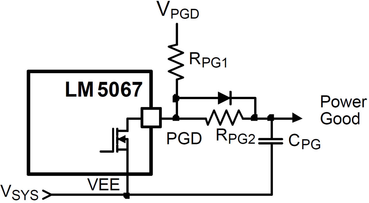
If a delay is required at PGD, suggested circuits are shown in the following figure. In Figure 9-13, capacitor CPG adds delay to the rising edge, but not to the falling edge. In Figure 9-14, the rising edge is delayed by RPG1 + RPG2 and CPG, while the falling edge is delayed a lesser amount by RPG2 and CPG. Adding a diode across RPG2. Figure 9-15 allows for equal delays at the two edges, or a short delay at the rising edge and a long delay at the falling edge.
 Figure 9-13 Adding Delay to the Power Good Output Pin - Delay Rising Edge Only
 Figure 9-15 Adding Delay to the Power Good Output Pin - Short Delay at Rising Edge and Long Delay at Falling Edge, or Equal Delays
 Figure 9-14 Adding Delay to the Power Good Output Pin - Long Delay at Rising Edge, Short Delay at Falling Edge