SCAS877F May 2009 – January 2016 CDCLVP1216
PRODUCTION DATA.
- 1 Features
- 2 Applications
- 3 Description
- 4 Revision History
- 5 Pin Configuration and Functions
-
6 Specifications
- 6.1 Absolute Maximum Ratings
- 6.2 ESD Ratings
- 6.3 Recommended Operating Conditions
- 6.4 Thermal Information
- 6.5 Electrical Characteristics: LVCMOS Input
- 6.6 Electrical Characteristics: Differential Input
- 6.7 Electrical Characteristics: LVPECL Output, at VCC = 2.375 V to 2.625 V
- 6.8 Electrical Characteristics: LVPECL Output, at VCC = 3 V to 3.6 V
- 6.9 Timing Requirements, at VCC = 2.375 V to 2.625 V
- 6.10 Timing Requirements, at VCC = 3 V to 3.6 V
- 6.11 Pin Characteristics
- 6.12 Typical Characteristics
- 7 Parameter Measurement Information
- 8 Detailed Description
- 9 Applications and Implementation
- 10Power Supply Recommendations
- 11Layout
- 12Device and Documentation Support
- 13Mechanical, Packaging, and Orderable Information
- 14Mechanical, Packaging, and Orderable Information
封裝選項
機械數(shù)據(jù) (封裝 | 引腳)
- RGZ|48
散熱焊盤機械數(shù)據(jù) (封裝 | 引腳)
- RGZ|48
訂購信息
7 Parameter Measurement Information
7.1 Test Configurations
Figure 5 through Figure 11 show how the device should be set up for a variety of test configurations.
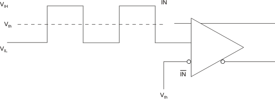
 Figure 6. DC-Coupled LVCMOS Input During Device Test
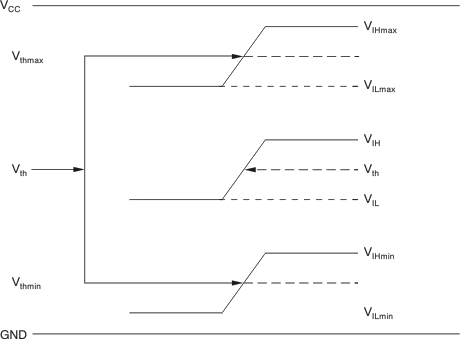
 Figure 7. Vth Variation over LVCMOS Vth Levels
 Figure 8. DC-Coupled LVDS Input During Device Test
 Figure 10. LVPECL Output DC Configuration During Device Test
 Figure 11. LVPECL Output AC Configuration During Device Test

